
Views: 0 Author: Site Editor Publish Time: 2026-08-24 Origin: Site


In semiconductor manufacturing, the structural integrity of a susceptor or carrier relies entirely on its protective layer. Microscopic deviations in this coating inevitably lead to macroscopic yield losses. Engineers apply Silicon Carbide (SiC) to high-purity graphite substrates using Chemical Vapor Deposition (CVD). This CVD process seals the porous substrate. It creates an impermeable barrier necessary to endure harsh chemical and thermal reactor conditions. However, not all coatings are equal. Evaluating a supplier requires looking far past surface-level marketing materials. You must meticulously verify exact thickness parameters, stringent uniformity tolerances, and the specific testing methodologies used by the manufacturer. Even minor inconsistencies can ruin a production batch. They alter thermal profiles or release contaminants directly into the chamber. We will explore the precise dimensional standards these components must meet. You will learn how to validate them to ensure consistent, high-yield manufacturing operations.
Optimal Thickness: Standard CVD SiC coatings typically range between 50 µm and 120 µm; exceeding this risks delamination, while falling short invites substrate outgassing.
Strict Uniformity: High-yield semiconductor applications require uniformity tolerances of ±10% (or tighter, e.g., ±5 µm) to maintain strictly controlled thermal gradients.
Evaluation Criteria: Reliable procurement relies on verifying vendor data through recognized metrology (e.g., SEM cross-sections, eddy current testing) and assessing CTE (Coefficient of Thermal Expansion) matching.
Failure Risks: Uneven coatings directly cause localized thermal spots, wafer slip in epitaxy, and premature part degradation in extreme plasma/chemical environments.
Coating specifications directly connect to bottom-line manufacturing metrics. You track defects per wafer diligently. You monitor chamber uptime constantly. You schedule component replacement frequencies to prevent unexpected breakdowns. All these operational metrics fluctuate based on coating performance. A flawed coating disrupts the entire production environment.
The SiC layer acts as a hermetic seal. Isotropic graphite is inherently porous by nature. If the protective coating thins or develops pinholes, the underlying graphite faces exposure. This exposure releases carbon dust into the reaction chamber. These impurities destroy the delicate crystal structure of the growing wafer. Contamination spikes defect rates and ruins entire production lots. A perfectly continuous layer prevents outgassing and contains substrate impurities entirely.
Uniformity dictates thermal conductivity across the component. In epitaxial growth or Metal-Organic Chemical Vapor Deposition (MOCVD), uneven coatings create micro-temperature variances. Silicon carbide transfers heat differently than the graphite core. When thickness fluctuates, thermal resistance fluctuates with it. These variances distort wafer deposition profiles. The film grows unevenly across the wafer surface. You lose critical yield due to poor thickness uniformity on the final semiconductor product.
Mission-critical Semiconductor Graphite Parts rely heavily on precise structural specs. They must survive corrosive precursor gases like hydrogen chloride (HCl) and ammonia (NH3). They operate in extreme heat, often sustaining temperatures between 1000°C and 1600°C. You cannot compromise on these structural details. A perfectly spec'd component withstands plasma etching and chemical attacks. A poorly coated part will fail prematurely, forcing unexpected chamber maintenance.
Many fabs only inspect parts for macroscopic cracks. They ignore micro-porosity. Always request porosity data from your vendor. Even invisible pores will trap process gases and release them during subsequent runs.
The semiconductor industry relies on a strict "Goldilocks" range for protective layers. We establish a baseline thickness for standard CVD SiC coatings. This usually falls between 50 µm and 120 µm. The exact ideal thickness depends heavily on the specific reactor type and component size. Barrel susceptors may require slightly different targets than single-wafer edge rings.
When the layer falls below 50 µm, we consider it critically thin. Thin coatings increase structural vulnerability significantly.
Pinholes and Micro-Cracking: Thin layers struggle to form a completely continuous lattice. They leave microscopic gaps.
Chemical Vulnerability: A thin layer provides an insufficient barrier against aggressive chemical etching. Process gases chew through the thin protection rapidly.
Reduced Lifespan: You will replace parts much more frequently. The harsh fab environment degrades thin coatings before standard maintenance cycles conclude.
Many process engineers hold a dangerous misconception. They believe thicker protection is always better. This is fundamentally false. A coating over 120 µm introduces severe thermomechanical risks.
Amplified Thermal Stress: Excessive thickness creates immense strain during rapid heating and cooling cycles. The thick layer cannot flex with the substrate.
CTE Mismatches: Graphite and SiC expand at slightly different rates. A thick coating exacerbates this Coefficient of Thermal Expansion (CTE) mismatch.
Catastrophic Failure: Extreme thickness often leads to spontaneous delamination. Sometimes, it causes catastrophic substrate cracking right in the middle of a process run.
You must specify exact ranges when ordering SiC Coated Graphite Parts to avoid both extremes. Precision matters more than sheer material volume.
Thickness Range | Structural Classification | Primary Fab Risks |
|---|---|---|
< 50 µm | Critically Thin | Pinholes, rapid chemical etching, outgassing. |
50 µm – 120 µm | Optimal (Standard) | Balanced thermal transfer, excellent chemical barrier. |
> 120 µm | Dangerously Thick | Delamination, high thermal stress, CTE mismatch cracking. |
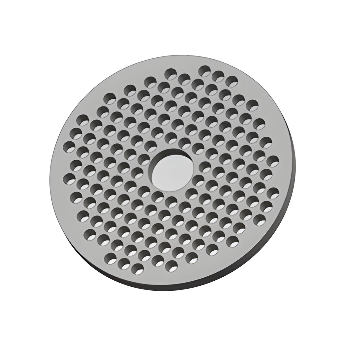
Average thickness means nothing if the coating fluctuates wildly across the surface. Top-tier components should demonstrate thickness variations of no more than ±5% to ±10% across the entire geometric surface. For highly sensitive nodes, engineers often demand absolute tolerances of ±5 µm. This prevents thermal anomalies during rapid thermal processing.
Maintaining uniformity poses a massive engineering challenge. Parts are rarely flat plates. We deal with susceptor pockets, edge rings, and deep alignment grooves. The CVD gas must flow evenly into every recess. If the gas flow stagnates in a deep groove, the coating grows too thick there. Suppliers must utilize highly optimized reactor designs. They use specialized rotation mechanisms to ensure uniform gas deposition on every complex surface.
Sharp edges act as magnets for CVD growth. Coating material naturally builds up faster on sharp corners. This phenomenon creates massive stress concentrations. These stress points act as the origin for severe micro-fractures. You must ensure proper substrate chamfering prior to the coating process. Radius design is critical. A rounded edge allows the SiC layer to wrap smoothly around the graphite core. Always verify that your supplier incorporates precision edge rounding before placing parts into the CVD chamber.
Do not accept a single thickness measurement. Demand a multi-point uniformity map. Suppliers should measure the center, middle radius, and extreme edges of the component to prove consistent deposition.
Procurement teams must move past glossy brochures. You need to scrutinize the raw data. Advise your engineering team on what to look for in technical datasheets. You must also know what details to question aggressively.
Examine the handling instructions and material properties carefully. Does the supplier list a vague "average thickness," or do they provide a guaranteed minimum and maximum? Look for specific testing standards. If a datasheet lacks details on how they measure uniformity, treat it as a major red flag.
Reliable vendors utilize sophisticated metrology to prove their claims. They employ both destructive and non-destructive methods.
Destructive Testing: Suppliers use cross-sectional Scanning Electron Microscopy (SEM). They sacrifice a sample part to view the microscopic layers. SEM provides exact layer thickness measurements. It also reveals the quality of the interface bonding between the graphite and the SiC.
Non-Destructive Testing (NDT): You cannot destroy every part you buy. NDT ensures batch consistency. Suppliers use eddy current testing to map thickness across the actual production parts. Ultrasonic inspection can also verify uniformity without sacrificing the component.
You must ask suppliers for hard data on thermal expansion alignment. The specific graphite grade must match the SiC layer perfectly. If the CTE curves diverge significantly at 1200°C, the part will fail. Request empirical charts showing the expansion rates of both materials from room temperature up to your maximum operating temperature.
Testing Method | Category | Primary Benefit | Limitation |
|---|---|---|---|
Scanning Electron Microscopy (SEM) | Destructive | Provides extreme detail of the bond interface. | Sacrifices the part; only tests a sample coupon. |
Eddy Current Testing | Non-Destructive | Allows 100% surface mapping of production parts. | Requires careful calibration for different geometries. |
Ultrasonic Inspection | Non-Destructive | Detects sub-surface voids and delamination early. | Struggles with highly complex or sharp edge areas. |
Even perfectly manufactured components carry operational risks. How you handle them dictates their ultimate lifespan. Fab technicians must understand the physical realities of these brittle materials.
The underlying graphite is relatively soft, but the SiC layer is incredibly hard and brittle. It behaves like glass. Even minor impact damage causes severe micro-fractures. Dropping a tool on the susceptor or bumping it against the chamber wall ruins the protective seal. Once the layer cracks, process gases immediately attack the exposed graphite. Technicians must use specialized handling tools and soft cleanroom padding.
Epitaxial processes involve continuous ramping. You take the part from room temperature up to beyond 1100°C rapidly. You then cool it down just as fast. This continuous ramping tests the limits of the coating uniformity over time. Fatigue accumulates. If the coating thickness varies, the thermal stress distributes unevenly. Over hundreds of cycles, these stressed areas develop hairline cracks. Uniformity directly delays the onset of thermal cycling fatigue.
Do not wait for a wafer defect to realize a part has failed. Implement rigorous baseline inspection protocols. Fabs should inspect parts visually under intense light before loading them into the chamber. Look for color variations that indicate thickness changes. Weigh the parts accurately. A sudden drop in mass over time indicates chemical etching or outgassing. Catching supplier anomalies early prevents catastrophic chamber contamination events.
Evaluating specialized fab components demands rigorous scrutiny. You must look far beyond standard material purity. Do not select suppliers based solely on their graphite grade. Demand verifiable thickness ranges and detailed uniformity maps. The protective layer dictates the entire success of the process.
Define strict acceptable ranges for your specific process, ideally keeping thickness between 50 µm and 120 µm.
Request batch-specific inspection reports using eddy current testing to guarantee ±10% uniformity.
Ask for sample coupons and perform in-house cross-sectioning (SEM) to verify interface bonding.
Establish strict cleanroom handling protocols to prevent micro-fractures before parts enter the reactor.
By enforcing these standards, you protect your reaction chambers, improve wafer temperature profiles, and secure higher yields across every production cycle.
A: Top-tier components require a typical variance expectation of ±10%. For highly sensitive epitaxial applications, engineers specify tighter absolute tolerances, often between ±5 µm and ±10 µm. This strict control prevents micro-temperature gradients and ensures consistent wafer deposition across the entire susceptor pocket.
A: While recoating is technically possible, it is rarely dimensionally stable. The initial process often etches the underlying substrate slightly. A second coating alters the original thermal profile and geometry. For high-precision semiconductor applications, this compromises thermal transfer and wafer uniformity, making recoating an unviable strategy.
A: Silicon carbide and graphite possess different thermal conductivities. If the protective layer thickness varies, it creates uneven thermal transfer pathways. This directly impacts wafer temperature uniformity. Localized thick spots act as thermal barriers, causing cold spots on the wafer during rapid thermal processing.


