
Views: 0 Author: Site Editor Publish Time: 2026-10-12 Origin: Site


Wafer yield is everything in compound semiconductor manufacturing. In the hyper-competitive landscape of advanced power electronics and high-brightness LEDs, a microscopic temperature variance or a single stray particle will ruin an entire production batch. Metal-Organic Chemical Vapor Deposition, commonly known as MOCVD, requires extreme heat and highly corrosive gas environments to function properly. Standard industrial materials simply fail under these unforgiving conditions.
Specialized semiconductor-grade carbon solves this exact problem. Serving as the foundational material for high-temperature processes, it ensures the stability and purity required for modern microelectronics. As an equipment engineer on the fab floor, you quickly realize that the quality of your reactor internals dictates your uptime. In this guide, we explore the intricate engineering behind susceptors, the absolute necessity of protective coatings, and the critical role of support carriers in maximizing epitaxy yield.
Ultra-High Purity: Semiconductor graphite is strictly engineered to maintain an ash content of less than 5 parts per million, preventing catastrophic wafer contamination during high-temperature crystal growth.
Thermal Uniformity: Precise MOCVD susceptors dictate the thermal distribution within the reactor chamber. Flawless CNC machining and high thermal conductivity remain fundamental requirements for high-yield epitaxy.
Essential Protection: Silicon Carbide coatings provide an impermeable barrier. This seals the naturally porous carbon structure, preventing corrosive gas degradation and eliminating particle shedding.
CTE Matching: Selecting the correct support trays requires exact Coefficient of Thermal Expansion alignment between the core and the coating to mitigate wafer bowing, thermal stress, or delamination.
The semiconductor industry is currently undergoing a massive structural transition. Foundries are aggressively scaling from 150mm to 200mm Silicon Carbide and Gallium Nitride wafers to meet booming demand from the electric vehicle and telecommunications sectors. What does this mean for process engineers? Larger wafers introduce an exponentially higher risk of thermal gradients across the substrate surface.
Recent industry analysis highlights that legacy thermal management setups are becoming the primary bottleneck for yield in these larger formats. Foundries are now forced to upgrade their reactor internals. They require ultra-precise carriers capable of maintaining absolute temperature uniformity across a much wider surface area. Sub-par thermal components are no longer just an inconvenience; they are a critical point of failure.
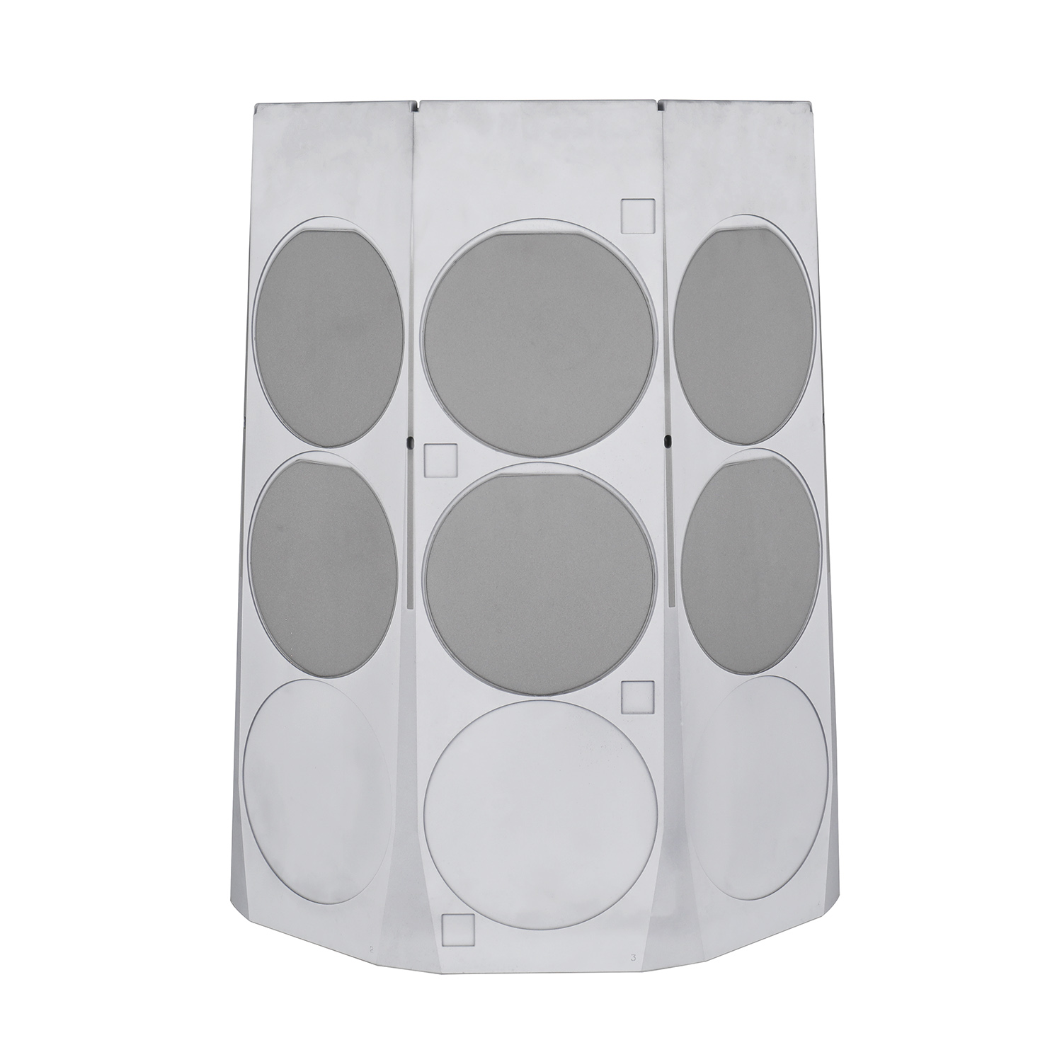
In the highly controlled environment of chip fabrication, standard industrial graphite is entirely inadequate. The physical, chemical, and thermal demands of advanced epitaxy require a specialized classification of material. Consequently, raw carbon must undergo rigorous processing to meet the empirical standards necessary for modern microelectronics.
The most critical distinction of this specialized material is its exceptional purity level. Standard industrial blocks often contain significant trace metals, including iron, copper, vanadium, and boron. If placed in a high-temperature MOCVD reactor, these impurities will volatilize. Should trace metals migrate into the epitaxial layer of a silicon or silicon carbide wafer, they create deep-level traps. These traps alter the electrical and optical properties of the final device, resulting in immediate batch failure.
To prevent such disasters, raw materials are subjected to extreme high-temperature halogen purification. Imagine standing next to a specialized purification furnace operating at temperatures exceeding 2,000 degrees Celsius. Halogen gases, typically chlorine and fluorine, pump into the chamber to react with metallic impurities. This forms volatile metal halides that are swiftly evacuated from the system. This meticulous process reduces the total ash content to less than 5 parts per million. Such extraordinary purity makes it the ideal Graphite Substrate for Crystal Growth, where even a single atomic flaw is unacceptable.
Standard carbon blocks are often extruded or die-molded. This manufacturing method results in an anisotropic structure where thermal and mechanical properties vary depending on the direction of measurement. In semiconductor applications, this inconsistency causes uneven thermal expansion, inevitably leading to severe wafer warpage.
In contrast, semiconductor-grade blocks are manufactured using cold isostatic pressing. Carbon powder is placed in a flexible mold and subjected to high-pressure fluid from all directions simultaneously. This creates a perfectly isotropic grain structure. Because the grain distribution is uniform, the resulting block behaves identically across the X, Y, and Z axes. When exposed to the aggressive thermal cycling of an MOCVD process, the material expands and contracts uniformly, providing a rock-solid foundation for delicate epitaxial layers.
Epitaxial deposition relies heavily on precise temperature control. High-purity isotropic carbon possesses exceptional thermal and electrical conductivity. This makes it an ideal material for radio frequency and induction heating systems.
The matrix efficiently absorbs electromagnetic energy, converting it into uniform heat. Thanks to high thermal conductivity, heat transfers rapidly and evenly across the surface to the wafers. This rapid thermal response time allows process engineers to execute precise temperature ramping and cooling protocols. These protocols are absolutely essential for forming distinct, high-quality atomic layers.
The MOCVD process serves as the foundational technology for manufacturing advanced power devices, RF amplifiers, and LEDs. At the very center of this complex process sits the susceptor. This highly engineered component directly dictates the success or failure of the deposition run.
Inside the reactor, the susceptor acts as the primary carrier and thermal interface for the substrates. Whether the recipe calls for sapphire, silicon, or Silicon Carbide wafers, the carrier holds them securely in precise positions. Meanwhile, reacting precursor gases flow over the substrates to deposit epitaxial layers.
These components must endure brutal environmental conditions. They are subjected to rapid thermal cycling, reaching temperatures between 1,000 and 1,200 degrees Celsius. They do this all while rotating at high speeds and fighting off chemical attacks from precursor gases. The mechanical integrity of the susceptor is a non-negotiable variable.
In the realm of epitaxy, temperature variance is the ultimate enemy of yield. A surface temperature deviation of just one or two degrees across the wafer can shift the emission wavelength of an LED by several nanometers. This pushes the final product out of the acceptable binning range.
To combat this, manufacturers utilize advanced CNC machining to achieve perfect thermal uniformity. The pockets holding the wafers are rarely perfectly flat. Instead, they are engineered with specific concavity or convexity measured in mere microns. This calculated curvature counteracts the natural bowing of the wafer at high temperatures. By maintaining continuous physical contact between the wafer and the pocket, heat transfer remains consistent. High-yield facilities rely on precision MOCVD Graphite Susceptors to mitigate thermal gradients and prevent crystal dislocations.
Modern reactors rely heavily on laminar gas flow to ensure the even deposition of atomic layers. If the gas flow becomes turbulent, the epitaxial thickness will vary across the batch, ruining the wafers.
Therefore, aerodynamic considerations are strictly integrated into the design. The surface must be exceptionally smooth, and the edges contoured to prevent flow separation. In planetary reactors, these carriers rotate at speeds often exceeding 1,000 RPM to average out spatial variations in gas concentration. The isotropic nature of the material ensures perfect balance during high-speed rotation, preventing micro-vibrations that could disrupt the delicate laminar gas boundary layer.
While ultra-pure isostatic carbon provides an ideal thermal foundation, the bare material cannot survive the internal environment of an MOCVD reactor on its own. To make it viable for advanced epitaxy, a specialized protective layer is strictly required.
By its inherent molecular nature, graphite is porous. Even high-density isostatic blocks contain microscopic voids. During deposition, corrosive gases such as ammonia and hydrogen chloride are utilized at temperatures exceeding 1,000 degrees Celsius.
If exposed to this environment, corrosive gases will infiltrate the pores and chemically etch the carbon structure from the inside out. This degradation generates deadly carbon dust. In a cleanroom environment, a single microscopic carbon particle landing on a wafer causes a killer defect, rendering the microchip useless. In addition, this porosity can trap precursor gases, leading to uncontrolled outgassing and unpredictable cross-contamination in subsequent runs.
To resolve these vulnerabilities, manufacturers apply a dense, impermeable layer of Silicon Carbide. Chemical Vapor Deposition is the industry standard method for this application.
During the coating process, precursor gases react at extreme temperatures to deposit a high-purity, crystalline layer directly onto the machined component. Unlike cheap spray coatings, this method creates a pinhole-free barrier that chemically bonds to the substrate. Integrating high-quality SiC Coated Graphite Parts into the reactor ensures exceptional chemical resistance, effectively halting degradation and particulate generation.
Applying a protective layer introduces a complex physical challenge known as thermal expansion mismatch. As the chamber heats up to 1,200 degrees Celsius and cools back down to room temperature, both the core and the coating will expand and contract.
If the Coefficient of Thermal Expansion of the underlying base does not precisely match that of the coating layer, thermal stress will cause the coating to micro-crack, blister, or completely delaminate. Once compromised, corrosive gases immediately attack the exposed carbon. Therefore, premium materials are specifically engineered with a thermal expansion rate that mirrors the coating, ensuring mechanical integrity over hundreds of rigorous thermal cycles.
Wafer processing does not end once the epitaxial layer is grown. Post-epitaxy processes, including rapid thermal annealing, oxidation, and dopant activation, require distinct thermal management strategies. In these downstream applications, the physical carrier holding the wafers must exhibit extraordinary thermal stability.
In MOCVD, the primary function of the carrier is to facilitate precise gas flow dynamics. However, in post-growth thermal processing, the operational requirements shift dramatically. Rapid Thermal Processing chambers subject wafers to extreme temperature ramps, often heating up at rates exceeding 50 to 100 degrees Celsius per second.
During these intense cycles, wafers must be supported by a carrier that absorbs and distributes heat instantaneously without introducing structural stress. Unlike standard quartz or ceramic boats, which may suffer from thermal shock, high-purity carbon offers an optimal balance of high thermal conductivity and low heat capacity. This allows the tray to heat and cool in near-perfect synchronization with the wafers, minimizing thermal lag that causes uneven dopant diffusion.
Annealing processes for advanced wide-bandgap semiconductors often demand temperatures exceeding 1,600 degrees Celsius. At these extreme thermal loads, conventional materials will soften, warp, or melt completely. Isostatic semiconductor-grade material, however, maintains its mechanical strength well beyond 2,000 degrees Celsius.
To prevent wafer warpage during these excursions, process engineers rely on a meticulously machined Graphite Support Tray for Epitaxy & Annealing. The structural flatness of the tray directly dictates the flatness of the wafer. If the carrier warps even slightly under extreme heat, the supported wafer experiences localized stress gradients, leading to slip-line defects or catastrophic breakage. Isotropic behavior ensures the tray remains perfectly flat, safeguarding the mechanical yield of the entire batch.
Parameter | Standard Industrial Graphite | Semiconductor Grade Graphite |
|---|---|---|
Ash Content (Purity) | > 500 ppm (High risk of metal contamination) | < 5 ppm (Ultra-pure, safe for epitaxy) |
Manufacturing Method | Extruded / Die-molded (Anisotropic) | Cold Isostatic Pressing (Isotropic) |
CTE Matching | Inconsistent, leads to coating delamination | Precisely tuned (4.0 - 5.0 x 10^-6 /°C) |
MOCVD Lifespan | Fails rapidly under corrosive gas attack | 6 to 12+ months with premium SiC coating |
Procurement managers frequently face pressure to reduce consumable costs. Substituting highly engineered components with cheaper alternatives introduces severe risks. The initial purchase price of consumables is only a fraction of the total Cost of Ownership. In a facility where a single fully processed wafer can be worth thousands of dollars, component-induced defects are unacceptably costly.
The most immediate consequence of using sub-par materials is wafer warpage. Inferior carriers are often machined with wider tolerances, resulting in pockets that fail to align with the wafer's high-temperature profile.
When a wafer does not sit perfectly inside the pocket, microscopic air gaps form. Because air is a poor thermal conductor, these gaps create localized cold spots across the substrate. This uneven thermal contact generates severe stress. As the layers grow, this stress manifests as bowing or slip-line dislocations, rendering the wafer entirely unsuitable for subsequent photolithography steps.
Cheaper components often utilize lower-grade coatings applied through inferior deposition methods. These protective layers frequently contain microscopic pinholes or suffer from poor thermal expansion matching.
During rapid heating and cooling cycles, mismatched expansion causes the low-grade coating to develop micro-cracks. Corrosive precursor gases penetrate these cracks, reacting with the underlying carbon to form methane and dust. This subsurface etching hollows out the base beneath the coating, eventually causing the protective layer to collapse. The resulting particulate contamination causes massive pinhole defects across the entire batch, dropping the yield rate to zero.
The degradation of sub-par components accelerates exponentially once the protective coating is compromised. High-quality parts are designed to withstand hundreds of thermal cycles and aggressive in-situ chemical cleaning processes. Low-density alternatives degrade rapidly under the same conditions.
When parts warp or begin shedding particles, they must be replaced immediately. Taking a multi-million-dollar reactor offline requires cooling the system, venting the chamber, replacing the part, pumping down to vacuum, and running calibration bakes. This unscheduled downtime can halt production for up to 24 hours. The lost revenue from a single day of reactor downtime vastly outweighs the initial savings of purchasing cheaper parts.
Mitigating the risks associated with thermal processing requires partnering with a manufacturer capable of meeting the stringent demands of the semiconductor industry. Evaluating suppliers goes beyond reviewing standard material data sheets. It requires a deep audit of their manufacturing capabilities and engineering expertise. Here are the standards you should demand:
Advanced CNC Machining Capabilities: The geometric complexity of pocket designs demands state-of-the-art machining infrastructure. A qualified manufacturer must utilize advanced multi-axis CNC machining centers capable of holding tolerances down to a few microns. Furthermore, they must employ Coordinate Measuring Machines and optical profiling to verify the exact concavity, convexity, and surface roughness of every single component before it moves to the coating phase.
In-House Purification and Coating: The highest quality control is achieved when a manufacturer controls the entire production lifecycle. Suppliers that rely on third-party vendors for purification or coating introduce unnecessary risks, such as exposing the porous material to atmospheric moisture during transit. Industry-leading suppliers operate vertically integrated facilities. This integration allows engineers to perfectly tailor the base material to the coating parameters, virtually eliminating the risk of delamination.
Customization for Specific Reactors: Equipment from major manufacturers utilize vastly different chamber dynamics. A susceptor designed for a high-speed rotation system requires different aerodynamics than a planetary reactor using satellite gas foil rotations. A premier manufacturer must have the engineering expertise to read complex schematics, reverse-engineer legacy components, and customize designs based on a foundry’s specific recipe.
Semiconductor-grade carbon is a critical variable in the modern chip-making equation. It is far more than just a simple consumable part; it is the thermal foundation upon which advanced microelectronics are built.
High-quality isostatic graphite ensures your wafers grow perfectly by providing unmatched thermal stability. Precise CNC machining prevents unwanted temperature gradients during production, while impermeable Silicon Carbide coatings block harmful corrosive gases effectively. This powerful synergy between ultra-pure materials and flawless engineering is what drives the successful fabrication of next-generation power chips and high-brightness LEDs.
Protect your wafer yield and reduce your total cost of ownership by making the right engineering choices. If you are upgrading your reactor for larger wafer sizes or struggling with yield inconsistencies, it is time to evaluate your thermal components. Partnering with a vertically integrated manufacturer ensures that every component inside your reactor is optimized for maximum performance. Explore the high-purity solutions at Harog to find the exact configuration tailored to your specific epitaxial recipe.
Lifespan varies heavily by the specific epitaxial process and cleaning protocols. However, a high-quality, coated susceptor typically lasts between six months to over a year. The lifespan is primarily dictated by the frequency of extreme thermal cycling and the aggressiveness of the in-situ chemical etching used to remove residual deposits between runs.
Silicon Carbide offers exceptional chemical resistance against highly corrosive precursor gases like ammonia and hydrogen chloride, which easily destroy bare carbon materials. Additionally, it possesses high thermal conductivity and can be engineered to precisely match the thermal expansion coefficient of the underlying base, preventing the coating from cracking under extreme heat.
Yes, these support trays are highly reusable and designed for longevity. However, they must undergo strict cleaning protocols between processing runs. This often involves high-temperature baking or specific chemical etching processes to remove any epitaxial deposits or dopant residues, ensuring zero cross-contamination for the next batch of wafers.
If impurities like iron, boron, copper, or aluminum are present in the base material, they can volatilize at high growth temperatures. These vaporized metals can then incorporate into the epitaxial layer of the wafer. This metallic contamination severely alters the electrical and optical properties of the semiconductor, leading to fatal defects and significantly lower production yields.
As wafer sizes increase to 200mm, the natural bowing of the substrate under high heat becomes significantly more pronounced. Susceptor pockets must be machined with a highly specific concave or convex profile to counteract this bowing. This ensures continuous physical contact, which is mandatory for eliminating thermal gradients and preventing edge-slip defects.
High-purity isostatic graphite itself can withstand temperatures well over 2,000 degrees Celsius. However, the operational limit is typically dictated by the protective coating. In a standard reactor environment, these coated components perform exceptionally well up to 1,600 degrees Celsius. Beyond this threshold, specific process conditions and gas chemistries must be carefully evaluated to prevent coating degradation.


