
Views: 0 Author: Site Editor Publish Time: 2026-06-08 Origin: Site


Modern semiconductor manufacturing faces harsh realities. As fabrication nodes shrink toward 3nm, thermal bottlenecks and particle contamination restrict wafer yield. You cannot ignore these primary limiters. Overcoming them requires materials capable of enduring extreme conditions. This is where high-purity semiconductor graphite becomes indispensable. It acts as a non-negotiable consumable for extreme-temperature environments. Fabs rely on it during processes reaching up to 1500°C. It also withstands highly corrosive chemical reactions. We must transition from basic material definitions to a technical procurement perspective. You need to know how to match specific graphite grades to distinct fabrication steps. Deciding between isotropic and extruded variations directly impacts your operational expenditures. We will explore how optimizing these choices improves wafer yield and controls supply chain costs. You will learn to navigate material specifications for maximum return on investment.
Application-Specific Selection: Advanced nodes require isotropic graphite with <10 ppm impurities, while extruded graphite offers a 20–25% cost reduction for less sensitive EDM (Electrical Discharge Machining) applications.
Yield & Thermal Stability: Synthetic graphite maintains structural integrity and delivers 120–150 W/mK thermal conductivity through aggressive 1500°C CVD (Chemical Vapor Deposition) thermal cycling.
Supply Chain Risks: Surging EV battery demand and energy-intensive production are causing price volatility; securing integrated suppliers (raw material + precision machining) is critical for semiconductor fabs.
Engineers cannot treat specialty carbon materials as generic commodities. You must match precise engineering applications to the correct material grade. Several critical fabrication steps rely entirely on these specialized components.
The Siemens process demands robust internal components. Engineers utilize graphite for polychucks and electrodes here. These parts withstand aggressive chemical deposition environments easily. They enable the safe, continuous production of ultra-pure polysilicon.
Moving to the Czochralski (CZ) crystal pulling process, the material serves multiple structural roles. High-purity heaters melt the raw silicon evenly. Crucible susceptors hold the quartz vessel securely. Surrounding thermal insulation prevents rapid heat loss. The entire CZ process relies on this stable hot zone. Without it, the silicon crystal boule develops fatal structural defects. Fabs avoid these micro-cracking risks by utilizing superior components.
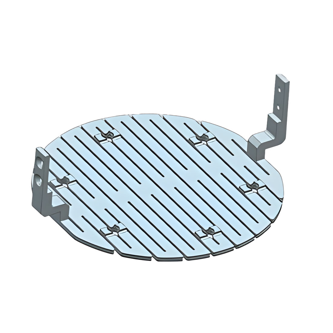
Epitaxy processes require absolute precision. Wafers receive thin crystalline layers during Metal-Organic Chemical Vapor Deposition (MOCVD). Fabs deploy SiC-coated graphite susceptors for this stage. The base material provides exceptional thermal transfer. The proprietary SiC coating seals porous surfaces perfectly. This seal prevents carbon dust from ruining delicate wafer layers.
Extreme thermal uniformity is another mandatory requirement. Uneven heating causes immediate wafer warping. It also creates costly edge defects. Advanced power electronics demand perfect epitaxial layers. Silicon carbide substrates are especially sensitive. The right susceptor guarantees flawless execution. It keeps yields high and scrap rates low.
Processing eventually moves to backend applications. High-density chips generate immense heat during standard operation. Industrial manufacturers use graphite cooling elements to manage this load. Custom heat sinks protect commercial data centers from thermal throttling. Cloud service providers install these components to reduce energy consumption. They also extend hardware lifespans significantly.
Emerging sectors push thermal boundaries even further. AI and quantum computing hardware require extreme temperature stability. Quantum bits fail under minor thermal fluctuations. Engineers rely on advanced thermal management solutions to maintain qubit integrity. Semiconductor graphite provides the necessary heat dissipation here.
Procurement and engineering teams need a direct evaluation framework. You must compare material specifications against process requirements. Over-specifying drains your budget. Under-specifying destroys wafer yields. We can break down the two primary grades.
Isotropic grades offer unmatched consistency. They deliver high thermal conductivity ranging from 120 to 150 W/mK. Manufacturers create this material using cold isostatic pressing. This method ensures identical thermal and mechanical properties in all directions. You get omnidirectional strength under extreme stress.
These specifications make it critical for precision CVD chambers. Crucibles also require uniform thermal expansion to prevent cracking. Market realities reflect this indispensability. Isotropic variants hold the dominant market share at approximately 37.6%. Advanced nodes simply cannot function without them. They remain the gold standard for front-end-of-line processes.
Extruded variants serve a different operational purpose. They feature lower thermal conductivity, typically between 80 and 110 W/mK. Their mechanical strength is optimized along the extrusion direction. You will notice weaker performance against perpendicular forces.
Despite these limitations, this grade remains highly viable. Engineers use it frequently for EDM electrodes. Specific heating elements also function perfectly using extruded materials. The business impact is substantial. It offers a 20–25% cost reduction compared to isotropic grades. We advise buyers not to over-spec materials blindly. If your process does not require isotropic uniformity, choose the extruded alternative. It saves money without compromising basic functionality.
Specification / Feature | Isotropic Graphite | Extruded Graphite |
|---|---|---|
Thermal Conductivity | 120–150 W/mK | 80–110 W/mK |
Directional Strength | Omnidirectional (Uniform) | Strongest along extrusion axis |
Primary Use Cases | CVD Chambers, CZ Crucibles | EDM Electrodes, Heating Elements |
Cost Impact | Premium Pricing | 20–25% Cost Reduction |
Technical specifications tie directly to operational expenditures. You must connect material purity to your return on investment. Smart procurement balances flawless performance against component costs.
Node Miniaturization Demands: We see node sizes shrinking continuously. Fabs require ultra-high purity materials. They specify >99.99% purity for 3nm and smaller nodes. This standard maintains CVD process integrity perfectly. Any foreign particle disrupts the nanometer-scale architecture. You cannot compromise on purity during advanced miniaturization.
The 10 ppm Threshold: Metallic impurities ruin entire wafer batches. You must respect the 10 ppm threshold. It acts as a strict ceiling for trace metals. Surpassing it causes catastrophic wafer contamination. Engineers observe this danger during 1500°C high-temp cycling. Metals vaporize and embed themselves into the silicon lattice. Keeping impurities below 10 ppm prevents this disaster.
Cost-Efficiency Scaling: We can establish a clear baseline assumption. You should not specify 99.99% purity for an application requiring only 99.5%. Standard EDM processes tolerate minor impurities easily. Artificially inflating specs here increases component costs by 15–30%. You must map the required purity level to the specific fabrication stage.
Chart: Purity Level vs. Cost Impact Matrix | |||
Process Sensitivity | Required Purity | Max Metallic Impurities | Cost Premium |
|---|---|---|---|
High (Epitaxy, CVD, 3nm Nodes) | >99.99% | <10 ppm | Baseline Premium (Highest) |
Medium (Standard Crystal Pulling) | 99.9% | <50 ppm | 10-15% Reduction |
Low (Standard EDM Machining) | 99.5% | <200 ppm | 15-30% Reduction |
Macro-level risks impact your daily operations. Lead times, pricing, and supplier reliability fluctuate wildly today. You must understand the external forces shaping the synthetic carbon market.
We face a significant supply chain threat. The electric vehicle (EV) sector overlaps heavily with our industry. A single EV battery requires up to 80kg of graphite for its anodes. This massive volume places immense strain on global synthetic production capacities. Fabs now compete directly with automotive giants for raw materials. This competition creates unpredictable lead times. It also drives structural price volatility.
Manufacturing high-purity components requires extreme heat. High-temperature graphitization is highly energy-intensive. Energy accounts for 30–40% of total production costs. Rising global electricity prices hit this sector hard. We also face a "green" paradox. Fabs want sustainable, low-carbon supply chains. However, traditional synthesis emits significant greenhouse gases. The industry is currently pushing toward low-carbon footprint synthesis. We see new purification methods emerging to solve this environmental challenge.
The market is shifting away from fragmented supply chains. Major manufacturers are acquiring precision machining facilities rapidly. They want to offer end-to-end solutions. This trend ensures better quality control. When one company handles synthesis and machining, traceability improves. They maintain trace-level quality control from powder to finished susceptor. This integration also reduces lead times substantially. Fabs prefer these consolidated partners to minimize procurement friction.
You need actionable criteria for vendor evaluation. Moving to the bottom of the procurement funnel requires strict diligence. Treat your supplier as a strategic yield-management partner.
When shortlisting a vendor for semiconductor graphite, implement the following checklist:
Verification of Purity: Never accept generic data sheets blindly. Does the supplier have in-house ash-content testing? Do they perform rigorous trace-metal analysis? They must guarantee <10 ppm impurities through certified internal lab results. Relying on third-party batch testing often causes delays.
Integrated Machining Tolerances: This material is notoriously brittle. Machining it requires specialized tooling and expertise. You should prioritize vendors who own the CNC machining process. Outsourcing to general machine shops leads to micro-fractures. Integrated vendors guarantee tighter tolerances and higher dimensional accuracy.
Coating Capabilities: Bare materials shed particles in vacuum environments. Check if the supplier offers proprietary coatings. SiC or Pyrolytic Carbon (PyC) coatings seal internal porosity effectively. These coatings extend component lifespans. They also prevent catastrophic particle shedding during sensitive epitaxy phases.
Sourcing these advanced materials requires strategic foresight. It is no longer just a routine raw material purchase. It operates as a critical yield-management strategy. Matching the exact material grade to the specific thermal environment prevents costly wafer scrap.
We advise engineering and procurement teams to act quickly. You should audit your current bill of materials today. Ensure you deploy isotropic and high-purity grades only where necessary. Leverage extruded grades safely where cost-savings make sense.
Take proactive steps to secure your supply chain. We encourage you to request a technical consultation with an integrated supplier. Download an updated material specification sheet. You can also submit a custom CAD file for a machining feasibility review to optimize your next production run.
A: Typically 99.99%, with metallic impurities strictly held below 10 ppm for front-end-of-line (FEOL) processes like CVD and epitaxy.
A: Isotropic graphite provides identical thermal and mechanical properties in all directions, ensuring uniform heat distribution and preventing micro-cracking under extreme thermal stress.
A: While CNTs offer superior strength and thermal properties for micro-electronic components, traditional high-purity synthetic graphite remains the only scalable, cost-effective material for large-format fabrication equipment like crucibles and susceptors.
A: Primarily energy costs (which make up 30-40% of production) and competing demand for graphitization capacity from the lithium-ion battery sector.


