
Views: 0 Author: Site Editor Publish Time: 2026-06-10 Origin: Site


Advanced semiconductor nodes, such as sub-3nm architectures, represent more than just a triumph of silicon engineering. They rely fundamentally on ultra-pure, thermally stable consumable materials. These materials ensure consistent yields during intense fabrication cycles. Without high-purity consumables, maintaining precise thermal gradients becomes impossible. Catastrophic contamination would quickly ruin delicate silicon wafers.
You can view semiconductor graphite as the critical backbone for wafer fabrication. It drives success in crystal growth and chemical vapor deposition (CVD) processes. Moving from basic research to high-yield fabrication demands careful material selection. You must understand the specific thermomechanical properties of different synthetic carbon types. We will map these variants directly to specific fab processes. You will learn how to evaluate suppliers based on strict purity thresholds. We will also explore strategies for long-term supply chain resilience. Read on to master the selection criteria for your fabrication environment.
Semiconductor graphite is an indispensable consumable in wafer fabrication, chosen for its extreme thermal survivability (sublimates above 3750°C) and high chemical inertness.
Isostatic graphite dominates advanced node manufacturing due to its isotropic structure and ultra-high purity, while extruded graphite offers a cost-effective alternative for less critical structural components.
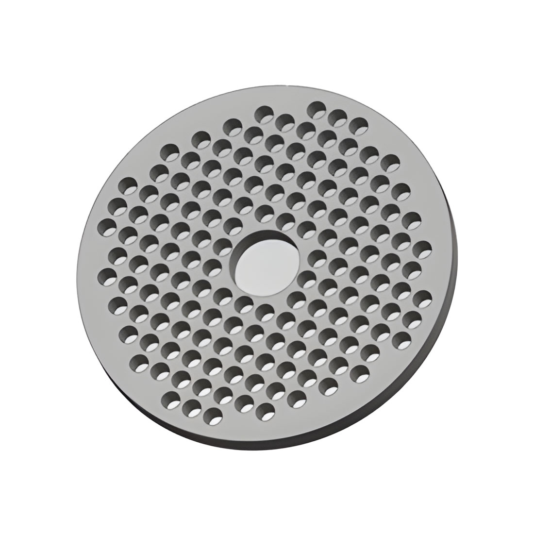
Core applications include monocrystalline silicon crucibles, CVD susceptors, high-purity etching electrodes, and heating elements.
Evaluating a graphite supplier requires strict verification of purity yields (often <10 ppm metallic impurities for advanced packaging) and precision machining tolerances.
High-temperature semiconductor processes rapidly degrade standard industrial materials. Annealing and epitaxy run at extreme thermal loads. When inferior materials break down, they cause catastrophic wafer contamination. This breakdown leads to massive yield loss. Fabrication facilities face a strict business problem here. They must maintain continuous operations without introducing foreign particles into the chamber. You need robust materials to survive these harsh environments.
The physical and chemical properties of synthetic graphite provide the exact evidence engineers need. First, consider its thermal resilience. Graphite lacks a traditional melting point. It plastically deforms around 2500°C. This deformation actually helps it absorb thermal shock without shattering. In inert environments, it directly sublimates above 3750°C. Very few materials can withstand these temperature extremes while maintaining dimensional stability.
Chemical inertness offers another major advantage. Semiconductor fabrication uses aggressive reagents. Hydrofluoric acid and nitric acid are common in these facilities. Synthetic graphite resists these harsh chemicals easily. It ensures structural integrity inside the reaction chamber. Standard metals would corrode instantly under these conditions. Corrosion releases metal ions. Metal ions destroy the electrical properties of the silicon wafer.
Thermal and electrical conductivity round out its core benefits. The crystalline lattice allows for rapid, uniform heat distribution. Uniform heat is highly critical for monocrystalline silicon growth. A common mistake is confusing this conductivity with semiconductor behavior. While it conducts electricity, it lacks a controllable bandgap. It acts as a passive heating element or structural support. It never acts as an active semiconductor device itself. It simply provides the perfect environment for silicon to grow.
Engineers must match the manufacturing process to the correct synthetic graphite classification. Selecting the wrong type introduces hidden risks. An evaluation framework helps buyers navigate these choices. We divide the solutions into two primary categories. You must weigh their structural properties against your specific process demands.
Manufacturers form this variant via Cold Isostatic Pressing (CIP). This sophisticated process applies equal pressure from all directions. The result yields an ultra-fine grain and high isotropy. Isotropic means it possesses uniform properties in all directions. You will not find weak points or directional bias in the material structure.
The performance metrics stand out clearly. It delivers high thermal conductivity, typically exceeding 100 W/m-K. It also features incredibly low thermal expansion, generally measuring under 4 ppm/K. These metrics prevent the material from expanding unevenly during rapid heating cycles.
You must apply a strict decision lens here. This material is absolutely mandatory for CVD chambers. You also need it for susceptors and sub-3nm node environments. Structural uniformity and ultra-purity remain non-negotiable in these zones. A single microscopic flaw can ruin an entire batch of advanced microchips.
Manufacturers form this variant via traditional extrusion. The mixture passes through a die under heavy pressure. This method results in coarser grains. It also creates directional properties, known as anisotropy. The material behaves differently depending on the axis you measure.
The metrics for extruded types differ from isostatic variants. It generally offers slightly lower thermal conductivity, ranging from 80 to 110 W/m-K. The mechanical strength is also lower along specific grain directions. However, it remains highly capable for many standard industrial uses.
Use a different decision lens for extruded materials. It works perfectly for Electrical Discharge Machining (EDM) electrodes. You can also use it safely for standard heating elements. It suits general metallurgical applications where anisotropic properties do not threaten wafer yield. Do not use it for delicate wafer support during epitaxy.
We can visualize the performance differences in the chart below.
Chart 1: Comparison of Isostatic and Extruded Properties | ||
Feature | Isostatic Graphite | Extruded Graphite |
|---|---|---|
Forming Process | Cold Isostatic Pressing (CIP) | Mechanical Extrusion |
Grain Structure | Ultra-fine, Isotropic | Coarser, Anisotropic |
Thermal Conductivity | > 100 W/m-K | 80 - 110 W/m-K |
Thermal Expansion | < 4 ppm/K (Uniform) | Directionally variable |
Primary Fab Use | CVD Chambers, Sub-3nm Nodes | EDM Electrodes, Heaters |
You must connect specific components to their operational success criteria in the fab. This feature-to-outcome mapping clarifies procurement needs. Each step of wafer fabrication requires distinct thermomechanical support. We rely on semiconductor graphite to fulfill these specialized roles.
The Czochralski (CZ) process demands extreme precision. The primary components here include massive crucibles and surrounding heating elements. The crucible holds molten silicon at incredibly high temperatures. The heaters provide the necessary thermal energy.
The outcome requires an ultra-pure, uniform thermal gradient. You need this gradient for flawless monocrystalline silicon growth. The crucible must not leach metallic impurities into the silicon melt. Any stray iron or copper particles will destroy the ingot. A high-quality crucible prevents this disaster completely.
Consider the core steps where this material interacts with crystal growth:
Melting: Heaters raise the chamber temperature above 1414°C to melt the raw polysilicon.
Stabilization: The crucible maintains a perfectly stable thermal environment without warping.
Seed Introduction: A silicon seed crystal dips into the melt while the thermal gradient remains steady.
Pulling: The system slowly pulls the growing ingot upwards while heat dissipates evenly through the isotropic structure.
Epitaxy involves growing a thin, highly controlled silicon layer on top of the wafer. The primary components used here are bases and susceptors. Suppliers often coat these susceptors with Silicon Carbide (SiC). The coating seals any microscopic pores on the surface.
This setup ensures extreme flatness during processing. It provides unmatched thermal stability during volatile gas-phase reactions. Uniform heat transfers from the susceptor directly to the wafer. This precision minimizes wafer warping. It also prevents unwanted thickness variations across the epitaxial layer.
Once engineers print the circuit patterns, they must etch the silicon. The primary components in this stage are high-purity electrodes. These electrodes sit inside the dry etching chamber. They endure constant bombardment from ionized gases.
The operational outcome focuses on plasma stability. The electrodes generate stable plasma environments necessary for precise cuts. They also prevent heavy metal contamination during these aggressive etching cycles. Lower-grade materials would erode quickly, showering the wafer with defect-causing particles. High-purity variants remain intact longer.
The semiconductor industry is shifting rapidly toward sustainable manufacturing. Fabs face immense pressure to reduce their environmental impact. High-density materials play a crucial role here. Their exceptional durability and reusability lower the overall replacement frequency. You consume fewer raw materials over a five-year operational window. This efficiency directly reduces the facility's carbon footprint. It also optimizes resource consumption without compromising yield.
Advancements in purification techniques extend these component life cycles even further. Modern facilities can achieve 99.99% or even 99.999% purity levels. Ultra-high purification removes volatile ash and trace metals. These metals normally accelerate oxidation and degradation. By eliminating them, the components survive many more thermal cycles. You replace them less frequently. This recyclability and extended lifespan support broader ESG (Environmental, Social, and Governance) goals.
Supply chain resilience presents another critical evaluation factor. The industry acknowledges ongoing geopolitical risks in raw material sourcing. High-quality needle coke and petroleum pitch are not universally available. You must mitigate these risks proactively. We recommend evaluating suppliers based on their vertical integration.
Look for the following resilience indicators when auditing a supplier:
Raw Material Control: They manage the process directly from raw coke and pitch down to the final component.
Localized Machining: They maintain CNC machining capabilities near your regional fabrication hubs.
In-House Purification: They do not outsource halogen purification to third-party vendors.
Buffer Stock Policies: They hold sufficient raw material reserves to survive sudden export restrictions.
Procurement teams face severe implementation risks if they choose the wrong vendor. The primary risk involves hidden metallic impurities. These impurities cause latent device failure. A microchip might pass initial quality checks but fail months later in the field. You must implement a rigorous evaluation checklist for all potential buyers. A strict vetting process protects your fabrication yields.
First, demand verifiable purity levels. You cannot trust marketing claims alone. Ask for explicit ash content and parts-per-million (ppm) certifications. Advanced nodes require metallic impurities to remain strictly below 10 ppm. Standard, older processes may accept up to 50 ppm. You must verify these numbers through independent laboratory testing reports.
Next, evaluate precision machining tolerances. The vendor must achieve near-net-shape processing. Susceptors feature ultra-tight dimensional geometries. Even a variance of a few microns can cause uneven gas flow in a CVD chamber. Uneven gas flow ruins the deposition layer. Ask vendors for their Cpk (Process Capability Index) data regarding complex geometries.
Finally, assess custom coating capabilities. Bare porous surfaces often generate microscopic particles. The supplier must demonstrate their ability to provide Silicon Carbide (SiC) or Pyrolytic Carbon (PyC) coatings. These coatings seal the porosity completely. They prevent particulate generation and block harsh chemical attacks.
Table 1: Supplier Vetting Checklist | ||
Criteria Area | Minimum Requirement | Red Flags to Avoid |
|---|---|---|
Purity Certification | <10 ppm for advanced nodes; 99.995%+ overall purity. | Refusal to share lab analysis; vague "high purity" claims. |
Machining Precision | Near-net-shape processing; proven tight dimensional tolerances. | Outsourced CNC routing; lack of coordinate measuring machines (CMM). |
Surface Coatings | In-house SiC or PyC coating capabilities. | Visible pinholes in sample coatings; poor adhesion test results. |
Traceability | Full lot traceability from raw coke to finished susceptor. | Inability to track raw material origins. |
Specifying the right consumable materials acts as a direct lever for improving wafer yield. Isostatic variants, in particular, provide the necessary isotropic properties for advanced fabrication. They maintain strict thermal stability during intense processing cycles. They also prevent the catastrophic contamination that ruins silicon ingots. You cannot compromise on these physical characteristics when pushing toward sub-3nm architectures.
Engineers and procurement teams should take immediate action based on these insights. Audit your current consumable lifespans to identify premature degradation. Request updated purity certifications from your existing vendors to ensure they meet the 10 ppm threshold. Schedule a technical consultation with an integrated supplier to review your custom geometries. By upgrading your semiconductor graphite requirements, you secure the reliability of your entire manufacturing operation.
A: No. While it conducts electricity due to its delocalized pi-electrons, it does not possess a controllable band gap (band structure). Therefore, it cannot be doped to act as a semiconductor. Rather, it remains an essential consumable material used to support semiconductor manufacturing processes.
A: Standard semiconductor processes typically require 99.99% purity. For advanced nodes (sub-3nm) and advanced packaging, the tolerance for metallic impurities drops strictly below 10 ppm (parts per million). High-temperature halogen purification achieves these extreme threshold requirements.
A: Isostatic graphite is pressed equally from all directions. This creates an isotropic structure with uniform thermal expansion and high density. This structure prevents warping and ensures even heat distribution across the wafer during delicate deposition processes. Extruded graphite's directional grain simply cannot guarantee this uniformity.


