
Views: 0 Author: Site Editor Publish Time: 2026-10-14 Origin: Site


Semiconductor-grade carbon demands rigorous Non-Destructive Testing, commonly referred to as NDT, to prevent internal microscopic flaws from triggering thermal inconsistencies or catastrophic particle contamination during wafer fabrication.
Ultrasonic testing methodologies, particularly Pulse-Echo and Phased Array systems, serve as the industry standard for mapping voids, micro-cracks, and density anomalies hidden deep within dense substrates.
For coated components, specialized high-frequency ultrasonic inspection is an absolute necessity. It identifies invisible delamination boundaries between the base material and the protective layer before the part enters the cleanroom.
Surface parameters must be meticulously engineered. Excessive roughness scatters acoustic waves and compromises diagnostic accuracy. Conversely, too smooth a finish risks coating adhesion failure under high thermal stress.
Strict cleanroom-grade handling and ultra-pure coupling protocols are mandatory before conducting acoustic tests. This ensures accurate signal transmission and eliminates the risk of introducing metallic impurities into the fab ecosystem.
Inside a modern wafer fabrication facility, the manufacturing environment is entirely unforgiving. The physical and thermal properties of equipment consumables directly dictate the yield and success of the entire process. Graphite is universally relied upon due to its exceptional thermal stability and resistance to corrosive plasma. However, the structural integrity of this material must be absolute. A microscopic variance that goes unnoticed can rapidly cascade into a multi-million dollar processing failure.
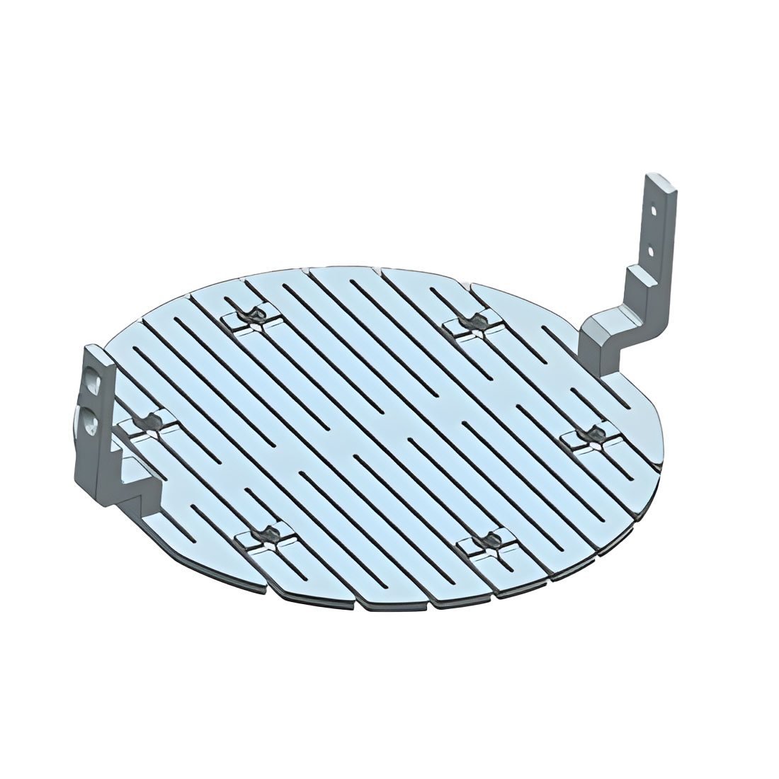
These robust components are the foundational backbone of extreme high-temperature semiconductor processes. In Metal-Organic Chemical Vapor Deposition and epitaxy reactors, susceptors are tasked with supporting and uniformly heating silicon or silicon carbide wafers to temperatures frequently exceeding 1000 degrees Celsius. Similarly, ion implantation systems depend heavily on specialized carbon parts to withstand high-energy plasma bombardment without degrading. Across all these applications, the component is subjected to brutal thermal cycling and highly reactive chemical gases. The operational lifespan and performance of Semiconductor Graphite Parts rely entirely on a uniform density matrix and a flawless internal structure. Any slight deviation alters thermal conductivity. This immediately translates to localized temperature spikes or drops across the wafer surface, causing fatal slip lines or uneven deposition.
Internal material defects pose severe, hidden risks to wafer yield. When a high-purity carbon component contains an internal void, that specific microscopic pocket acts as a thermal insulator. During rapid thermal processing, this localized insulation forces uneven heat distribution. Consequently, the wafer resting on the susceptor experiences a harsh temperature gradient. This gradient can trigger severe wafer warpage, inconsistent film deposition thicknesses, or erratic dopant diffusion profiles. Because these dangerous anomalies are entirely subterranean, they completely evade standard optical or visual inspections. This operational reality makes advanced acoustic diagnostics not just an option, but a strict manufacturing necessity.
To guarantee internal perfection and safeguard the fabrication process, quality assurance engineers deploy sophisticated ultrasonic testing. This method utilizes high-frequency acoustic sound waves to safely penetrate the dense material, effectively mapping its hidden internal geometry. Depending on the specific thickness, density, and physical shape of the component, technicians will select from several distinct acoustic techniques.
Pulse-Echo testing remains the foundational workhorse of industrial inspection. In this setup, a single transducer acts as both the transmitter and the receiver of the acoustic energy. When the technician applies the probe to the susceptor, a precise burst of high-frequency sound penetrates the dark, granular matrix. When this wave encounters a physical boundary, such as the back wall of the component or a hidden internal void, the acoustic energy reflects back to the probe. By calculating the exact microsecond it takes for the echo to return, the oscilloscope displays the precise depth of the defect. This technique is exceptionally reliable for verifying part thickness and pinpointing planar defects oriented parallel to the testing surface.
In contrast to dense aerospace metals, carbon substrates are inherently porous and highly attenuating. They aggressively absorb sound energy. For thicker ingots or susceptors, the standard Pulse-Echo method often struggles to receive a readable return signal. The sound wave simply runs out of energy before it can bounce back. In these challenging scenarios, Through-Transmission Testing is deployed. This configuration utilizes two independent transducers positioned on opposite sides of the component. One fires the acoustic wave, while the other listens for it. If an internal micro-crack blocks the direct sound path, the receiving probe registers a sudden drop in signal amplitude. While highly effective at penetrating thick materials, this method only reveals the lateral location of a flaw, not its exact depth.
For components featuring complex, multi-tiered geometries, Phased Array Ultrasonic Testing represents the absolute pinnacle of diagnostic technology. Unlike conventional probes that emit a single, rigid sound beam, a phased array probe houses multiple individual piezoelectric elements. Driven by sophisticated software, these elements pulse independently in microsecond sequences. This allows the operator to electronically steer, sweep, and focus the acoustic beam across various angles without physically moving the probe. The resulting data generates a highly detailed, medical-grade cross-sectional image of the component interior.
Inspection Method | Typical Frequency | Best Application | Primary Limitation |
|---|---|---|---|
Pulse-Echo | 1 to 5 MHz | Thin to medium parts, depth measurement | Struggles with highly porous or very thick ingots |
Through-Transmission | 0.5 to 2 MHz | Thick blocks, highly attenuating materials | Cannot determine the exact depth of the defect |
Phased Array | 2 to 10 MHz | Complex geometries, 3D defect mapping | Requires expensive equipment and highly trained operators |
Industry Trend Analysis: Looking at the broader trajectory of the semiconductor industry, the relentless migration toward sub-3nm and 2nm nodes is fundamentally reshaping non-destructive testing requirements. At these microscopic scales, the tolerance for thermal variance has essentially vanished. Forward-looking fabs and premium suppliers are rapidly transitioning from manual pulse-echo spot checks to fully automated, robotic phased array systems. Furthermore, integrating machine learning algorithms to filter out acoustic noise is becoming the new standard. This creates highly accurate digital twins of the components, ensuring every micrometer of the material matrix is accounted for before it ever enters the cleanroom.
While raw isostatically pressed carbon is highly resilient, it is routinely coated to suppress particulate generation and dramatically enhance chemical resistance against etching gases. Inspecting these advanced composite components introduces a complex new layer of difficulty to the testing workflow.
In cutting-edge semiconductor nodes, stray particle contamination is the leading culprit behind catastrophic device failure. Bare carbon substrates, despite their high density, can easily shed microscopic dust when subjected to harsh vacuum plasma or mechanical friction. To neutralize this threat, manufacturers seal the part with a dense, highly crystalline layer of Silicon Carbide applied via Chemical Vapor Deposition. This process yields a pristine, chemically inert shield. Ensuring the absolute integrity of SiC Coated Graphite Parts is non-negotiable. A single breach in this armor directly exposes the sterile cleanroom to fatal carbon contamination.
Imagine a susceptor spinning at high speeds during an epitaxial growth cycle. If a hidden micro-gap exists between the carbon base and the protective silicon carbide layer, the intense thermal stress will inevitably cause the coating to buckle, blister, and flake off. This separation, known as delamination, is the most critical failure mode for coated components. Ultrasonic testing is uniquely equipped to hunt down these invisible boundary failures. Technicians deploy specialized, ultra-high-frequency ultrasonic waves frequently exceeding 15 MHz. These waves are meticulously calibrated to focus entirely on the microscopic interface between the substrate and the coating layer. If the protective layer is perfectly fused to the base, the sound wave transitions smoothly into the deeper material. Conversely, if even a micrometer-thin air gap exists, the acoustic energy reflects violently back to the monitor. Catching these adhesion failures on the manufacturing floor saves fabs from devastating downtime.
In the highly specialized realm of acoustic diagnostics, the physical texture of a component exterior plays a pivotal role. Managing Graphite Surface Roughness requires engineers to navigate a delicate, precise balance between operational functionality and testing accuracy.
Ultrasonic inspection fundamentally relies on the seamless transfer of acoustic energy from the probe into the solid medium. This transfer requires a liquid couplant to displace any air between the transducer and the part. When the exterior roughness, measured as Ra or Rz, is too coarse, the microscopic peaks and jagged valleys on the surface trap tiny, stubborn air bubbles. Because high-frequency sound waves cannot travel through air, these trapped pockets act as an acoustic brick wall, scattering the ultrasonic beam in multiple directions. On the diagnostic monitor, this diffuse scattering manifests as erratic background noise. This acoustic interference drastically lowers the signal-to-noise ratio, effectively camouflaging the subtle echoes produced by actual internal micro-cracks.
Manufacturers face a distinct engineering paradox. The bare carbon substrate must retain a specific degree of mechanical roughness to allow the subsequent coating to physically anchor itself during the high-temperature deposition process. If the surface is polished to a flawless mirror finish to guarantee perfect ultrasonic signal coupling, the coating will lack the necessary mechanical grip and peel off under thermal stress. Conversely, if left too abrasive, ultrasonic inspection becomes highly unreliable. To solve this, premium manufacturers utilize precision CNC machining and proprietary lapping techniques to achieve an optimized roughness threshold. Typically, an Ra value hovering between 1.0 and 3.2 micrometers is the sweet spot. This exact baseline ensures robust, permanent bonding while remaining smooth enough to permit clear, low-noise acoustic wave propagation during quality assurance.
Fundamentally, semiconductor-grade carbon behaves very differently under acoustic stress than homogeneous aerospace metals. The inherent microstructural grain boundaries and slight microporosity introduce significant diagnostic hurdles that require specialized engineering approaches.
Unlike the tight, uniform crystalline lattice of steel or aluminum, which allows sound waves to travel vast distances with minimal energy loss, graphite retains a granular matrix. As acoustic waves traverse this material, the mechanical energy is rapidly scattered by grain boundaries and absorbed by microscopic pores. This phenomenon is known as acoustic attenuation. Consequently, a standard ultrasonic signal can quickly weaken and vanish entirely before it ever reaches the back wall of a thick susceptor. Operators often have to meticulously adjust the gain on their oscilloscopes, balancing the need to push the sound wave through the thick material against the risk of amplifying irrelevant background noise.
To defeat acoustic attenuation, technicians must carefully manipulate their equipment, focusing heavily on transducer frequency selection. There is an inescapable inverse relationship in acoustic physics. Higher frequencies provide stunning resolution for finding microscopic defects but suffer from terrible penetration depth. Lower frequencies easily punch through thick, porous materials but sacrifice the ability to resolve tiny anomalies. Inspecting dense fab components requires a calculated compromise. Technicians typically utilize broadband, lower-frequency transducers ranging from 1 to 5 MHz paired with high-gain amplifiers. This optimized setup pushes the sound wave deep into the material while maintaining just enough resolution to flag critical internal voids.
Because these components are destined for ultra-pure cleanrooms, the procedures surrounding the testing process itself must adhere to uncompromising purity protocols. A flawless part can easily be ruined by improper testing environments.
Before a transducer ever makes contact, the component must undergo meticulous preparation. Any residual machining fluids, ambient dust, or human skin oils will immediately interfere with the ultrasonic couplant, generating false positive readings or entirely blocking the sound wave. Furthermore, the selection of the couplant is highly regulated. Standard industrial ultrasonic gels are packed with trace minerals, halogens, and sulfur. These elements act as fatal dopant contaminants in a semiconductor fab. Therefore, testing facilities strictly utilize ultra-pure Deionized water as the coupling medium. Post-inspection, the parts are subjected to a rigorous vacuum baking process to outgas any residual moisture trapped within the micro-pores, ensuring the substrate is bone-dry before vacuum sealing.
Despite their ability to withstand thousands of degrees, these carbon components are mechanically brittle at room temperature. Improper physical handling during the inspection process can actually induce the very micro-cracks the test is designed to find. To ensure parts are cleaned and handled in a fab environment safely, technicians outfitted in full lint-free garments must use specialized vacuum wands or custom-molded, non-marring polymer cradles to maneuver the heavy susceptors. Applying concentrated point loads or using rigid metal clamps during automated scanning can chip the delicate edges. By utilizing automated robotic scanning arms, testing facilities can map the entire geometry without subjecting the part to damaging physical stress.
Ultimately, the reliability of your wafer fabrication process is inextricably linked to the strength of your supply chain. For procurement managers and fab engineers, sourcing consumable parts that have not undergone comprehensive internal inspection introduces an unacceptable level of operational risk.
When evaluating a manufacturing partner for critical fab consumables, buyers should demand absolute transparency and strict baseline parameters. A premium supplier will readily provide comprehensive documentation for every batch. From an engineering standpoint, you should look for raw material density greater than 1.85 grams per cubic centimeter, apparent porosity under 8 percent, and ash content strictly below 5 ppm. Procuring components from a supplier that outsources its ultrasonic testing introduces unnecessary logistical delays and quality blind spots. Manufacturers equipped with robust, in-house capabilities can integrate quality control at multiple critical stages of production.
Acoustically scanning the raw carbon block before machining ensures that no expensive CNC time is wasted milling a defective blank. Testing the part again after machining, and a final time after the coating is applied, creates a closed-loop quality assurance ecosystem. Every shipment must be accompanied by detailed ultrasonic C-scan digital maps proving the absence of internal voids or coating delamination. By partnering with manufacturers who treat acoustic testing as a mandatory, non-negotiable science, fabs can secure high-purity components that consistently survive the extreme rigors of modern semiconductor processing.
Ultrasonic testing stands as the ultimate safeguard for verifying the internal integrity of semiconductor consumables. By deploying advanced acoustic methodologies, fabs can detect invisible voids, prevent catastrophic coating delamination, and avoid devastating wafer yield losses. Mastering the delicate balance between surface roughness, coating adhesion, and defect detection directly translates to highly stable thermal processing and significantly lower operational costs. To maintain a competitive edge and secure top-tier components tailored to your specific reactor requirements, explore the engineered solutions available at https://en.harog.net and partner with a supplier who embeds rigorous, in-house testing protocols into their manufacturing DNA.
Yes, ultrasonic methodologies are highly adaptable for both stages of production. For raw, uncoated blocks, technicians utilize lower-frequency transducers typically 1 to 3 MHz to penetrate the dense, porous material and identify internal voids, density gradients, or deep macro-cracks. Once the component is finished, high-frequency ultrasonic waves often 5 MHz and above are deployed specifically to inspect the boundary interface. This high-frequency scanning is critical for ensuring perfect bonding and detecting any microscopic delamination between the carbon substrate and the protective layer.
No, ultrasonic testing is strictly categorized as a non-destructive methodology. The process relies on the transmission of high-frequency acoustic waves that pass through the atomic lattice of the material. These sound waves do not alter the physical dimensions, chemical composition, or structural integrity of the component. The only potential risk during testing is the introduction of chemical contaminants from improper couplants or moisture retention. However, by strictly utilizing deionized water and enforcing rigorous post-inspection vacuum baking protocols, manufacturers eliminate any risk of contamination or structural degradation.
Surface roughness creates a severe acoustic impedance mismatch at the boundary layer. When ultrasonic sound waves transition from the liquid couplant into the solid material, a rough exterior traps microscopic air pockets and acts as an irregular acoustic lens. This scatters the directional sound waves, reducing the total amount of energy that successfully penetrates the component. Consequently, this scattering generates excessive background noise on the diagnostic monitor, severely reducing the signal-to-noise ratio and making it exceedingly difficult for technicians to identify the subtle echoes produced by legitimate internal micro-defects.
The minimum detectable flaw size is dictated by the frequency of the transducer, the inherent density of the specific material grade, and the depth of the flaw. As a general rule of acoustic physics, a system can detect defects that are roughly half the size of the ultrasonic wavelength being used. In highly dense, isostatically pressed material, advanced phased array systems operating at optimized frequencies can reliably detect internal voids, inclusions, and micro-cracks as small as 0.3 to 0.5 millimeters in diameter.
Comprehensive ultrasonic inspection must be performed by the manufacturer on 100 percent of the components prior to delivery. Once installed in the fab, the testing frequency depends entirely on the operational environment. For components subjected to extreme thermal cycling and harsh plasma environments such as MOCVD susceptors, fabs may implement periodic inspection during scheduled preventive maintenance windows. This ongoing inspection helps identify heat-induced micro-cracking or progressive coating delamination before it leads to catastrophic particle generation and subsequent wafer contamination.
An A-scan provides a one-dimensional view, displaying the amplitude of the ultrasonic signal against time. It is primarily used by technicians to pinpoint the exact depth of a single defect at a specific point. In contrast, a C-scan generates a two-dimensional, top-down graphical map of the entire component. By stitching together thousands of A-scan data points, the C-scan provides a comprehensive visual representation of the internal structure, making it much easier to identify the overall size, shape, and distribution of flaws or delamination zones.
Yes, but it requires highly specialized equipment. Because protective coatings applied via Chemical Vapor Deposition are incredibly thin, usually ranging from 80 to 120 micrometers, standard ultrasonic frequencies cannot distinguish the top surface echo from the substrate interface echo. To measure coating thickness accurately, engineers must utilize ultra-high-frequency transducers, often exceeding 20 MHz, paired with precision delay lines. This allows the system to resolve the two distinct acoustic boundaries and calculate the exact thickness of the protective layer across the entire part.


